Atmel ATA6617 LIN 系統級封裝(SiP)解決方案

Atmel公司的ATA6617是一款系統級封裝(SIP)解決方案,在單個QFN 5mm × 7mm 封裝中整合了ATA6624 LIN 系統基礎芯片 (system basis chip, SBC) 與AVR微控制器 (ATtiny167),其中ATA6624 LIN SBC 包含LIN收發器、穩壓器和看門狗。采用這種系統級封裝解決方案,客戶只需一塊IC就能夠創建完整的LIN節點。本文介紹了ATA6617主要特性,系統應用框圖以及ATA6617–EK開發板主要特性和電路圖。
本文引用地址:http://www.j9360.com/article/196691.htmATA6617是一款系統級封裝(SIP)解決方案,在單個QFN 5mm × 7mm 封裝中整合了 ATA6624 LIN 系統基礎芯片(system basis chip, SBC) 與AVR微控制器(ATtiny167),其中ATA6624 LIN SBC 包含 LIN 收發器、穩壓器和看門狗。采用這種系統級封裝解決方案,客戶只需一塊IC就能夠創建完整的LIN節點。新器件基于愛特梅爾的第二代LIN IP,具有出色的EMC和ESD性能,專為低成本LIN從節點應用而優化,并包含一個功能強大的в屑成硬件程序的LIN UART,可將LIN的代碼量減少到約1 kB 閃存,并把中斷發生p到最少。
ATA6617主要特性:
вLIN SBC
LIN收發器,同類最佳電磁兼容(EMC)性能
LIN、Wake和Supply (VS) 引腳上ESD級別更高
線性低壓降穩壓器
Window看門狗
符合LIN 2.0和SAE J2602-2標準
вAVR微控制器
16 Kbyte閃存
硬件LIN UART
11路單端/ 8路差分10位 ADC
512-Byte 真正EEPROM
512-Byte內部SRAM
低功耗模式
多種定時器
主要優點
PCB 尺寸要求最小
產品易于使用
降低總體系統成本
由于LIN協議處理不占用資源,目標應用擁有最大 CPU 資源和閃存
應用:
汽車
工業
醫療
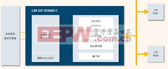
圖1. ATA6617系統應用框圖
ATA6617 – EK Development Board V1.1
The development board for the ATA6617 IC is designed to give designers a quick start with the ATA6617 IC and to enable prototyping and testing new LIN designs.
The ATA6617 is a dual-chip System-in-Package (SIP) product, which is particularly suited for complete LIN bus slave and master node applications. It supports highly integrated solutions for in-vehicle LIN networks. The first chip is the LIN-system-basis-chip (LIN SBC) ATA6624, which has an integrated 5V voltage regulator, a window watchdog, and a fully integrated LIN transceiver, in compliance with the LIN specification 2.1. The second chip is an automotive microcontroller from Atmel’s series of AVR 8-bit microcontrollers with advanced RISC architecture (ATtiny167 with 16K flash). All pins of both integrated chips are bonded out to provide customers the same flexibility for their applications as they have when using discrete parts.
ATA6617–EK 開發板特性:
All Necessary Components to Put the ATA6617 in to Operation Are Included
Placeholders for Some Optional Components for Extended Functions Included
All Pins Easily Accessible
Easily Adaptable Watchdog Times by Replacing a Single Resistor
Possibility to Activate an External NPN-transistor to Boost the Output Current of the Voltage Regulator (Jumper JP3)
Possibility to Select between Master or Slave Operation (Mounting D2 and R1)
Possibility to Mount an External Quartz to Handle Time-critical Applications (Not Necessary for LIN Communication)
Push Button Included to Create a Local Wake-up after Entering Sleep or Silent Mode
Ground Coulter Clip for Connecting Probes when Measuring with the Oscilloscope
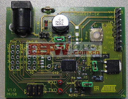
圖2. ATA6617 – EK 開發板外形圖
ATA6617 - EK Development Board
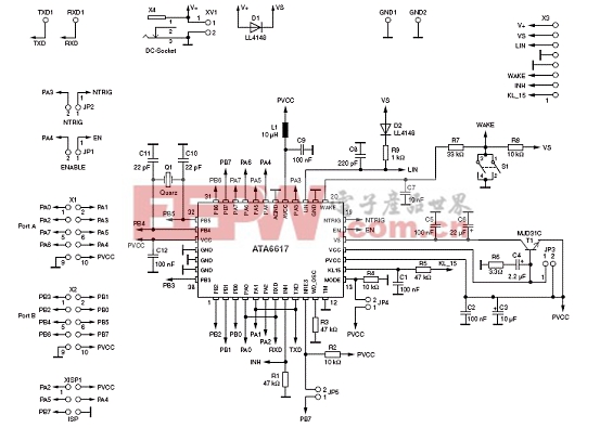
圖3.ATA6617–EK 開發板電路圖


評論